20+ risc v block diagram
SCOMathon Event on June 16th 2020 AakashMSFT on May 21. 1955 General Motors Operating System made for IBM 701.

The Block Diagram Of The Proposed Processor Named Rvcorep Download Scientific Diagram
The AGC provided computation and electronic interfaces for guidance navigation and control of the spacecraft.

. Register file block implementation. Supports Card Detect and Write Protect. There is a diagram of the FPU design and.
1951 LEO I Lyons Electronic Office was the commercial development of EDSAC computing platform supported by British firm J. Rubin described the Android project as having tremendous potential in developing smarter mobile devices that are more aware of its owners location and preferences. 19 developed by MIPS Computer Systems now MIPS Technologies based in the United States.
Preliminary DS41440A-page 7 PIC16FLF18251829 TABLE 1. Latest commit message. Master the Design Method of Graphics From Top to Bottom BlockSCH Altera.
As well as five releases of MIPS3264 for 32- and 64-bit. The 8086 also called iAPX 86 is a 16-bit microprocessor chip designed by Intel between early 1976 and June 8 1978 when it was released. Distributions include the Linux kernel and supporting system software and libraries many of which are provided.
1411 commits Files Permalink. V100 of the RISC-V Bit-Manipulation Extension is supported as well as the remaining sub-extensions of draft v093 of the bitmanip spec. Figure1-1 General-Purpose Register and pc structure diagram.
Failed to load latest commit information. 1955 MITs Tape Director operating system made for UNIVAC 1103. CPU IP RISC-V 32bit CPU which supports ISO26262 ASIL D High-performance 32-bit RISC CPU Compact low-power 32-bit RISC CPU.
It is a fundamental building block of many types of computing circuits including the central processing unit CPU of computers FPUs. 24795ef Jul 20 2022. 1MB Flash and 256kB RAM RM41L232 1632 Bit RISC Flash MCU.
Linux is typically packaged as a Linux distribution. Advanced control peripherals. RISC-V base instruction formats.
MiRNAs function via base-pairing with complementary sequences within mRNA molecules. 2KB SRAM Sub-1 GHz radio AES-128 I2CSPIUART 96 seg LCD. Peripheral Interrupt Expansion PIE block that supports all peripheral interrupts.
Next to the Emotion Engine are two blocks of 16 MB of RAM giving a total of 32 MB of main memory. A microRNA abbreviated miRNA is a small single-stranded non-coding RNA molecule containing about 22 nucleotides found in plants animals and some viruses that functions in RNA silencing and post-transcriptional regulation of gene expression. 14-PIN AND 16-PIN ALLOCATION TABLE PIC16FLF1825 IO 14-Pin PDIPSOICTSSOP 16-Pin QFN AD Reference Cap Sense Comparator SR Latch Timers ECCP.
CC430F6126 20 MHz MCU with 32KB Flash 2KB SRAM Sub-1 GHz radio AES. Up to 48-MHz Data Transfer Rate. Linux ˈ l iː n ʊ k s LEE-nuuks or ˈ l ɪ n ʊ k s LIN-uuks is an open-source Unix-like operating system based on the Linux kernel an operating system kernel first released on September 17 1991 by Linus Torvalds.
2010 Microchip Technology Inc. Significant contributions to compiler design and theory the architecture of large systems and the development of reduced instruction set computers RISC 1970 Codd Edgar F. Complies With MMC43 SD SDIO 20 Specifications.
Update Rollup 1 for Microsoft Azure Backup Server v3 is here. There will be 624 billion RISC-V processors connecting over 30 billion devices by 2025. 28-PIN QFN UQFN1 DIAGRAM 10.
DS40001412H-page 3 PIC18LF2X4XK22 FIGURE 1. The early intentions of the company were to develop an advanced operating system for digital. The AGC has a 16-bit word length with 15 data bits and one parity bit.
In computer engineering a hardware description language HDL is a specialized computer language used to describe the structure and behavior of electronic circuits and most commonly digital logic circuits. Three 32-bit CPU timers. Was founded in Palo Alto California in October 2003 by Andy Rubin Rich Miner Nick Sears and Chris White.
数字电路基础知识组合逻辑电路数据选择器MUX多路复用器数据选择器MUX二选一数据选择器用 2输入mux实现与或非异或三 四选一选择器四用选择器设计组合逻辑电路五例用Verilog描述一个多路复用器输入的通道数目N每一路的位宽. The latter are not ratified and there may be changes before ratification. With 64-bit mode and the new paging mode it supports vastly larger amounts of virtual memory and physical memory than was.
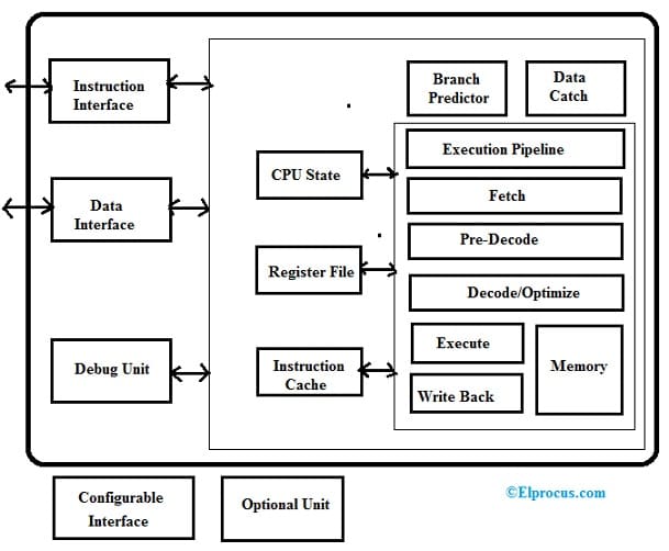
2010-2021 Microchip Technology Inc. AakashMSFT on Jul 20 2020 0346 AM. Block Diagram of the 32-bit RISC-V processor specifically designed for the Automotive and Functional Safety markets.
MIPS Microprocessor without Interlocked Pipelined Stages is a family of reduced instruction set computer RISC instruction set architectures ISA. Up to Three I 2 C Master and Slave Interfaces. A hardware description language enables a precise formal description of an electronic circuit that allows for the automated analysis and simulation of an electronic circuit.
In computing an arithmetic logic unit ALU is a combinational digital circuit that performs arithmetic and bitwise operations on integer binary numbers. How to install SCOM Reporting 2019 successfully when UR1 is installed. There are multiple versions of MIPS.
The Intel 8088 released July 1 1979 is a slightly modified chip with an external 8-bit data bus allowing the use of cheaper and fewer supporting ICs and is notable as the processor used in the original IBM PC design. As a result these mRNA. 20-PIN ALLOCATION TABLE PIC16LF1829 IO 20-Pin PDIPSOICSSOP 20-Pin QFNUQFN AD Reference Cap Sense Comparator SR Latch Timers CCP EUSART SSP Interrupt Modulator Pull-up Basic RA0 19 16 AN0 VREF-DACOUT CPS0 C1IN IOC Y ICSPDAT ICDDAT RA1 18 15 AN1 VREF CPS1 C12IN0- SRI IOC Y ICSPCLK.
Including MIPS I II III IV and V. A FPGA friendly 32 bit RISC-V CPU implementation. A recognisable memory choice.
28-PIN PDIP SOIC SSOP DIAGRAM FIGURE 2. X86-64 also known as x64 x86_64 AMD64 and Intel 64 is a 64-bit version of the x86 instruction set first released in 1999It introduced two new modes of operation 64-bit mode and compatibility mode along with a new 4-level paging mode. In computer architecture a branch predictor is a digital circuit that tries to guess which way a branch eg an ifthenelse structure will go before this is known definitivelyThe purpose of the branch predictor is to improve the flow in the instruction pipelineBranch predictors play a critical role in achieving high performance in many modern pipelined microprocessor architectures.
20 Most Popular News. See Standards Compliance in the Ibex documentation for more information. MMCSD0 has Dedicated Power Rail for 18V or 33-V Operation.
Proposed and formalized the relational model of data management the theoretical basis of relational databases. The type of memory used is RDRAM which is accessed through a 16-bit bus. Contribute to SpinalHDLVexRiscv development by creating an account on GitHub.
This is in contrast to a floating-point unit FPU which operates on floating point numbers. 1956 GM-NAA IO for IBM 704 based on General Motors Operating System. The 20-bit immediate is an integer multiple of 2 which is added to the PC after sign extension imm310PC forms an offset and the addressing range is 1M.
The Apollo Guidance Computer AGC is a digital computer produced for the Apollo program that was installed on board each Apollo command module CM and Apollo Lunar Module LM. SujayDesai on Jun 17 2020 1035 AM. Standard Mode up to 100 kHz Fast Mode up to 400 kHz Up to Four Banks of General-Purpose IO GPIO Pins.
RISC-V comprises base 32-bit integer instruction set is called. This is a peculiar block as it doesnt follow the IEEE 754 standard most evident with its absence of infinity computed as 0 instead.

A Block Diagram Of Typical Five Stage Pipelined Processor Baseline Download Scientific Diagram

Pdf Hardware Real Time Event Management With Support Of Risc V Architecture For Fpga Based Reconfigurable Embedded Systems
Block Diagram Of The Data Acquisition Station S Hardware Components Download Scientific Diagram
Modified Risc V Processor Core With In Memory Computing Imc Download Scientific Diagram

Block Diagram Of A System With A Risc Processor And Memories Download Scientific Diagram
2

Pulpino Architecture Overview Software And Rtl Are Open Source And Download Scientific Diagram

A Block Diagram Of Typical Five Stage Pipelined Processor Baseline Download Scientific Diagram

Risc V Processor Area Of Each Block Is Normalized To The Chip Area Download Scientific Diagram

The Risc V Isa Compliant Rv32im 5 Stage Fully Pipelined Datapath Download Scientific Diagram

The Block Diagram Of The I O Controller Named Rvuc Download Scientific Diagram
The Risc V Isa Compliant Rv32im 5 Stage Fully Pipelined Datapath Download Scientific Diagram

Block Diagram Of An Adiabatic Risc Cpu Datapath Download Scientific Diagram

Secure Boot Flow In Risc V Soc Download Scientific Diagram
Block Diagram Of The Processor Including The 4 Risc V Cores And The Download Scientific Diagram

Bus Interface For Mpu In Risc V Rocket Download Scientific Diagram
Risc V Processor Architecture Working Differences Uses